Electron hole

An electron hole is one of the two types of charge carriers that are responsible for creating electric current in semiconducting materials. A hole can be seen as the "opposite" of an electron. Unlike an electron which has a negative charge, holes have a positive charge that is equal in magnitude but opposite in polarity to the charge an electron has.[2]
Holes can sometimes be confusing as they are not physical particles in the way that electrons are, rather they are the absence of an electron in an atom. Holes can move from atom to atom in semiconducting materials as electrons leave their positions.[2] An analogy may be helpful. Imagine people standing in a line, on a set of steps. If the person at the front of the line goes up one step, that person leaves a hole. As everyone steps up one step the available step (the hole) moves down the steps.
Holes are formed when electrons in atoms move out of the valence band (the outermost shell of the atom that is completely filled with electrons) into the conduction band (the area in an atom where electrons can escape easily), which happens everywhere in a semiconductor.
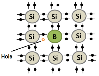
In order to encourage hole formation semiconductors are doped with certain elements. These semiconductors, where holes are the most prominent charge carrier, are known as p-type.[2] When an element that has one less electron in its outer shell than silicon, such as boron, is added into a crystalline structure of silicon it replaces one of the silicon atoms in the crystalline structure.[3] This can be seen in Figure 1. These holes readily accept free electrons and complement n-type semiconductors as the excess electrons of the n-type can be absorbed by the p-type. This property is integral to the p-n junction, a vital component in the operation of a diode and photovoltaic cells. Electrical conductivity is drastically increased with either the production of extra electrons or holes.[4]
Both electrons and holes are vital to the creation of current in semiconductors. Under the influence of some external voltage, both electrons and holes can move through a semiconducting material. This process is known as applying a forward or reverse bias.[4]
For more in-depth information on this concept, click here or here.
For Further Reading
For further information please see the related pages below:
- Semiconductor
- Metal
- Photovoltaic cell
- Diode
- Charge carrier
- Or explore a random page!
References
- ↑ Created internally by a member of the Energy Education team. Adapted from: HyperPhysics. (August 20, 2015). P and N-Type Semiconductors [Online]. Available: http://hyperphysics.phy-astr.gsu.edu/hbase/solids/dope.html
- ↑ 2.0 2.1 2.2 Margaret Rouse. (August 17, 2015). What is a Hole? [Online]. Available: http://whatis.techtarget.com/definition/hole
- ↑ Tomas Markvart. Solar Electricity, 2nd ed. Chichester, West Sussex, England: John Wiley & Sons, 2000
- ↑ 4.0 4.1 HyperPhysics. (August 17, 2015). Electrons and Holes [Online]. Available: http://hyperphysics.phy-astr.gsu.edu/hbase/solids/intrin.html#c4

